Linear and digital integrated circuits lab questions
Linear and digital integrated circuits lab questions
The following texts are the property of their respective authors and we thank them for giving us the opportunity to share for free to students, teachers and users of the Web their texts will used only for illustrative educational and scientific purposes only.
All the information in our site are given for nonprofit educational purposes
The information of medicine and health contained in the site are of a general nature and purpose which is purely informative and for this reason may not replace in any case, the council of a doctor or a qualified entity legally to the profession.
Linear and digital integrated circuits lab questions
1.Define an Integrated circuit.
An integrated circuit(IC) is a miniature ,low cost electronic circuit consisting of active and passive components fabricated together on a single crystal of silicon.The active components are transistors and diodes and passive components are resistors and capacitors.
2.What are the basic processes involved in fabricating ICs using planar technology?
1.Silicon wafer (substrate) preparation
2.Epitaxial growth
3.Oxidation
4.Photolithography
5.Diffusion
6.Ion implantation
7.Isolation technique
8.Metallization
9.Assembly processing & packaging
3.List out the steps used in the preparation of Si – wafers.
1.Crystal growth &doping
2.Ingot trimming & grinding
3.Ingot slicing
4.Wafer policing & etching
5.Wafer cleaning
4.Wwrite the basic chemical reaction in the epitaxial growth process of pure silicon.
The basic chemical reaction in the epitaxial growth process of pure silicon is the hydrogen reduction of silicon tetrachloride.
1200oC
SiCl4 + 2H2 <> Si + 4 HCl
5.What are the two important properties of SiO2?
1.SiO2 is an extremely hard protective coatng & is unaffected by almost all reagents except by hydrochloric acid. Thus it stands against any contamination.
2.By selective etching of SiO2 , diffusion of impurities through carefully defined windows in the SiO2 can be accomplished to fabricate various components.
6.Explain the process of oxidation.
The silicon wafers are stacked up in a quartz boat & then inserted into quartz furnace tube. The Si wafers are raised to a high temperature in the range of 950 to 1150oC & at the same time, exposed to a gas containing O2 or H2O or both.The chemical action is
Si + 2H2O > Si O2+ 2H2
7.What is meant by molecular beam epitaxy(MBE)?
In the molecular beam epitaxy, ilicon along with dopants is evaporated.The evaporated species are transported at a relatively high velocity in a vacuum to the substrate.The relatively low vapour pressure of silicon & the dopants ensures condensation on a low temperature substrate.Usually, silicon MBE is performed under ultra high vacuum (UHV) condition of 10-8 to 10-10 Torr.
8.What are the advantages of Molecular Beam Epitaxy( MBE )?
( i ) It is a low temperature process, useful for VLSI. This minimises outdiffusion & autodoping.
( ii ) It allows precise control of doping& permits complucated profiles to be generated.
( iii )Linear doping profile desirable for varactor diode in FM , can be obtained with MBE.
( iv )Wider choice of dopants can be used.
9. What are oxidation induced defects in semi conductor?
1.Stacking faults
2.Oxide isolation defects
Stacking faults:
Structural defects in the silicon lattice is called oxidation induced stacking faults.The growth of stacking faults is a strong function of substrate orientation , conductivity type & defect nuclei present.The stacking faults formation can be suppressed by the addition of HCl.
Oxide isolation defects :
The stress along the edges of an oxidised area produce severe damage in the silicon. Such defects results in increased leakage in nearby devices.High temperatures (around 950oC ) will prevent stress induced defect formation.
10.What is bird’s beak?
In local oxidation process, the oxidation of silicon proceeds slightly under the nitride as well. Also, a large mismatch in the thermal expansion co-efficients of Si3N4 &
Silicon results in damage to the semi conductor during local oxidation.This damage can be graetly reduced by growing a thin layer of SiO2 prior to placement of the Si3N4 mask.
Typically 100 to 200Ao is used for this puspose. Unfortunately, this greatly enhances the penetration of oxide under the nitride masked regions , resulting in oxide configurations called bird’s beak.
11.What is lithography?
Lithography is a process bywhich the pattern appearing on the mask is transfered to the wafer.It involves two steps: the first step requires applying a few drops of photoresist to the surface of the wafer & the second step is spinning the surface to get an even coating of the photoresist across the surface of the wafer.
12.What are the different types of lithography? What is optical lithography?
The different types of lithography are :
1.Photolithography
2.Electron beam lithography
3.X ray beam lithography
4.Ion beam lithography
Optical lithography:
Optical lithography comprises the formation images with visible or UV radiation in a photoresist using contact, proximity or projection printing.
13.What are the two processes involved in photolithography?
- Making a photographic mask
- Photoetching
The development of photographic mask involves the preparation of initial artwork and its reduction , decomposition of initial artwork or layout into several mask layers.
Photoetching is used for the removal of SiO2 from desired regions sothat the desired impurities can be diffused.
14.Distinguish between dry etching & wet etching.
Dry etching |
Wet etching |
1.Gaseous mixture is used as the chemical |
Chemical reagents used are in the liquid form. |
2.Smaller line openings(≤ 1μm) are |
Line opening are larger.(> 1μm) |
3.It produces straight walled etching process. |
It produces patterns with undercutting. |
15.What is meant by reactive plasma etching?
The term reactive plasma is meant to describe a discharge in which ionization & fragmentation of gases takesplace& produce chemically active plasma species, frequently
oxidizers and reducing agents.Such plasmas are reactive both in the gas phase & with solid surfaces exposed to them.When these interactions are used to form volitile products so that material is removed or etching of material form surfaces that are not masked to form lithographic patterns , the technique is known as reactive plasma etching.
16.What are isotropic & anisotropic etching processes?
Isotropic etching is a wet etching process which involves undercutting.
Aisotropic etching is a dry etching process which provides straight walled patterns.
17.Define diffusion.
The process of introducing impurities into selected regions of a silicon wafer is called diffusion. The rate atwhich various impurities diffuse into the silicon will be of the order of 1μm/hr at the temperature range of 900oC to 1100oC .The impurity atoms have the tendency to move from regions of higher concentrations to lower concentrations.
18.What is dielectric isolation?
In dielectric isolation, a layer of solid idelectric such as SiO2 or ruby completely surrounds each components thereby producing isolation , both eletrical & physical.This isolating dielectric layer is thick enough so that its associated capacitance is negligible.Also, it is possible to fabricate both pnp & npn transistors within the same silicon substrate.
19.What are the advantages of ion implantation technique?
- It is performed at low temperature.Therefore, previously diffused regions have a lesser tendency for lateral spreading.
- In diffusion process, temperature has to be controlled over a large area inside the oven, wheras in ion implantation process,accelerating potential & beam content are dielectrically controlled from outside.
20.What is metallization?
The process of producing a thin metal film layar that will serve to make interconnection of the various components on the chip is called metallization.
Unit II
1.What are the advantages of ICs over discrete circuits.?
- Minimization & hence increased equipment density.
- Cost reduction due to batch processing.
- Increased system reliability
- Improved functional performance.
- Matched devices.
- Increased operating speeds
- Reduction in power consumption
2. What is OPAMP?
An operational amplifier is a direct coupled high gain amplifier consisting of one or more differential amplifiers , followed by a level translator and an output stage.It is a versatile device that can be used to amplify ac as well as dc input signals & designed for computing mathamatical functions such as addition, subtraction , multiplication, integration & differentiation.
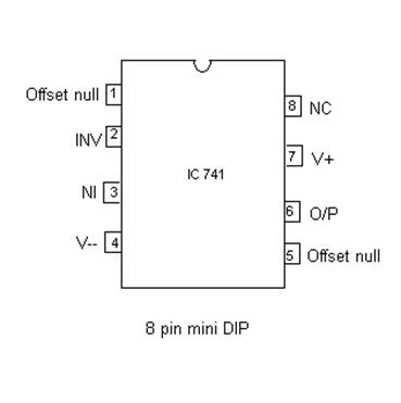
3.Draw the pin configuration of IC741.
4. List out the ideal characteristics of OPAMP?
( i )Open loop gain, AOL =
(ii)Input impedance,Ri=
(iii)Output impedance,Ro=
(iv)Bandwidth,Bw=
(v)Zero offset,ie,Vo=0 when V1=V2=0
5.what are the different kinds of packages of IC741?
a)Metal can (TO) package
b)Dual-in-line package
c)Flat package or flat pack
6.What are the assumptions made from ideal opamp characteristics?
i)The current drawn by either of the input terminals(non-inverting/inverting) is negligible.
ii)the potential difference between the inverting & non-inverting input terminals is zero.
7.What is a precision rectifier ?
A rectifier circuuit built with opamps and a few diodes for half wave/full wave signal rectification is called a precision rectifier.
Cut in voltage of a precision rectifier =Vd /AOL
Where Vd=knee voltage
AOL=openloop voltage gain
8)What are the applications of diodes in opamp circuits?
- Half wave rectifier
- Full wave rectifier
- Clipper
- Clamper
- Peak detector
- Log & antilog amplifiers
9)What are the different types of filters?
Based on functions: Low pass filter,High pass filter,Band pass filter,
Band reject filter
Based on order of transfer function: first ,second,third higher order filters.
Based on configuration: Bessel,Chebychev,Butterworth filters.
10.What is an instrumentation amplifier?
To amplify the low level output signal of the transducer so that it can drive the indicator or display is the major function of the instrumentation amplifier.It is used for precise,low level signal amplification where low noise,low thermal and time drifts,high input resistance & accurate closed loop gain are required.
11.What are the different features of Instrumentation amplifier?
1.High gain accuracy
2.High CMRR
3.High gain stability
4.Low dc offset
5.Low output impedence
12.Define input bias current & input offset current.
Input bias current:
It is the average value of base currents entering into the terminals of OPAMP.
IB+ - IB-
IB = -----------------
2
Input offset current :
The absolute value of the difference between the base currents IB+ & IB-
is called input offset current.
│ IOS│ = IB+ - IB-
13.What is input offset voltage?
Due to unavoidable imbalances inside the OPAMP, the output voltage may not be zero eventhough bias current & offset current compensation are provided. So, a small voltage must be applied at the input terminals to make the output voltage zero.This voltage is called input offset voltage VOS.
14.Define thermal drift.
The bias current , offset current & offset voltage change with temperature. A circuit carefully nulled at 25oC may not remain so when the temperature raises to 35oC.This is called thermal drift . Often, offset current drift is expressed in nA/ oC and offset voltage drift in mV/ oC.
15.Define CMRR.
The relative sensitivity of an OPAMP to a difference signal as compared to a common mode signal is called the common mode rejection ratio (CMRR) & it gives the figure of merit ρ for the differential amplifier.
CMRR, ρ = │ Ad / Ac │
Ad à Differential mode gain
Ac à Common mode gain
CMRR is expressed in Db .Higher the value of CMRR, better is the OPAMP
16.Define supply voltage rejection ratio(SVRR)
The change in OPAMP’s input offset voltage due to variations in supply voltage is called the supply voltage rejection ratio.It is also called Power Supply Rejection Ratio(PSRR) or Power Supply Sensitivity(PSS).
17.Define Gain BW product.
It is the bandwidth of the OPAMP when the voltage gain is unity.It is also called closed loop BW, unity gain BW & small gain BW.
18.What is a voltage follower?
The circuit in which the output voltage follows the input voltage both in magnitude & phase is called the voltage follower circuit.It is a non-inverting amplifier with infinite input resistance & zero feedback resistance.
19.What are the applications of 555 Timer ?
- astable multivibrator
- monostable multivibrator
- Missing pulse detector
- Linear ramp generator
- Frequency divider
- Pulse width modulation
- FSK generator
- Pulse position modulator
- Schmitt trigger
20. What are the advantages of LM 723?
- The output voltage can be adjusted & set at a wide range of both positive/negative regulated voltages.
- It has current limit protection
- Current folback can be implemented.
Unit III
1. What is the main feature of CMOS circuits?
The main feature of CMOS is that both n- channel and P- channel is fabricated
on the same substrate.
2. Write down the procedure for designing the transistor circuitry for CMOS logic
circuit?
The procedure for designing the transistor circuitry for CMOS logic can be
summarized by the following step.
- Construct the logic diagram using basic AOI or OAI structuring deeper nesting such as OAOI and AOAI is allowed. Deeper nesting OAOI and AOAI is allowed.
- Use the gate nFET relations to construct the nFET logic circuit between the output and ground.
- To obtain the topology of the pFET array, start with the original logic diagram and push the bubble back toward the input using the DeMorgan’s rules. Continue the backward pushing until every input is bubbled. The pFET circuitry between the output and VDD is then obtained.
3. What is a bistable circuit?
A bistable circuit is one that can store ( or hold) either a logic 0 or logic1
indefinitely ( or atleast as long as power is applied ).
4. What are the three operational modes of the SRAM?
SRAMS have three operational modes. They are hold, write and read. When the
cell is in hold state, a value of the bit is stored in the cell for future use. During a
write operation, a logic 0 or 1 is fed to the cell for storage. The value of the stored
bit is transmitted to the outside world during a read operation.
5. What is static noise margin?
The static noise margin is the separation between the curves along a 45o slope in
the drawing and has unit of volts.
6. How are SRAM arrays obtained?
Static RAM arrays are created by replicating the basic storage cell and adding
the necessary peripheral circuitry.
7. What is floating gate?
A reprogrammable ROM array is built using special FETs that use a pair of
stacked poly gates. The top most gate constitutes the usual gate terminal of the
transistor. However, another poly gate layer is sandwitched in between the top
poly and silicon substracts. It is not electrically connected to any part of the
transistor or auxillary circuitry and is therefore called as electrically floating gate.
8. What is fan-in?
The number of inputs to a logic gate is called the fan-in (FI).
9. Explain RAM.
- RAMs has the basic unit called binary cell.
- The binary cell can store either 1 or 0 indefinitely, as long as the power is ON.
- Data can be written into RAM as read out from RAM. The previously stored
data can be erased and new data can be written into RAM.
- Hence it is called as READ write memory.
- When power supply is switched OFF, all the binary cells gets erased.
10. What are the different types of RAM?
The different types of RAM are :
i) Nos RAMs ( Nitride metal oxide semiconductor RAMs)
ii)CMOS ( complementary metal oxide semiconductor RAMs)
iii) Schottky TTL RAMs
iv) ELL RAMs.
11. What is the procedure followed to store a new word in memory?
The procedure followed for transferring a new word to be stored into memory
are as follows:
i) Apply the binary address of the desired word to the address lines.
ii) Apply the data bits that must be stored in memory to the data input lines.
iii) Activate the write input : The memory will then take the bits from the input data lines and store them in the word specified by the address line.
12. What is the procedure followed to take the word out of memory?
The procedure followed is as follows:
i) Apply the binary address of the desired word to the address lines.
ii) Activate the read input.
The memory input will then take the bits from the word that has been selected by
the address and apply them to the output data lines.
13. What is memory enable?
Memory enable ( sometimes called as the chip select) is a control input, which is
used to enable the particular memory. When the memory enable is inactive, the
memory chip is not selected and no operation is performed. When the memory
enable input is active, the read/write determines the operation to be performed.
14. What is access and cycle time?
The access time of a memory is the time required to select a word and read it.
The cycle time of a memory is the time required to complete a write operation.
15. How does the read write input determine the type of operation?
If read write is 1, the memory performs a read operation symbolized by the
statement,
Dataout ---- Mem [ Address];
If read write is 0, the memory performs a write operation symbolized by the
statement,
Mem [Address]----- DataIn;
16. Explain SRAM.
– It is an operating mode.
-- Static RAM ( SRAM) consists od internal latches that stores the binary
information.
- The stored information remains valid as long as power is applied to the
unit.
- SRAM is easier to use and has shorter read and write cycles.
17. Explain DRAM.
– the dynamic RAM (DRAM) is am operating mode, which stores the binary
information in the form of electric charges on capacitors.
- The capacitors are provided inside the chip by MOS transistors.
- The stored charge on the capacitors tend to discharge with time and the
capacitors must be periodically recharged by refreshing the dynamic memory.
- Refreshing is done by cycling through the words every few milliseconds to
restore the decaying charge.
- DRAM offers reduced power consumption and larger storage capacity in a
single memory chip.
18. Differentiate volatile and non- volatile memory.
Volatile memory Non- volatile memory
i) They are memory units which lose i) It retains stored information when
stored information when power is power is turned off.
turned off.
ii) Example: ii) Example:
SRAM & DRAM. Magnetic disk & ROM.
19. What is the use of two- dimensional decoding? Give an example.
Two- dimensional decoding is used to arrange the memory cells in an array in
the form of a square.
For example: A decoder with K inputs and 2k outputs requires AND gates
with K inputs per gate. The total number of inputs per gate can be reduced by
employing two decoders in a two- dimensional selection scheme. It will result in
two K/2 – input decoders instead of one K- input decoder. One decoder performs
the row selection and the other the column selection.
20. What is meant by a non- destructive readout?
Each memory location contains one byte of data. When a byte is read from the
memory, it is not destroyed, but remains in the memory. This process of
“copying” the contents of a memory without destroying the contents is called non
destructive readout.
Unit IV
1)What is the process of constructing ICs?
The ICs are constructed in a series of steps viz
- silicon wafer growth.
- Wafer cutting, polishing.
- Doping.
- Oxidation
2)How the individual layers are formed ?
The layers are formed y oxidation, implantation of dopants and masking .
3) What is the use for oxidation layer?
The Sio2 layer known as oxide layer or oxidation is formed by selective reduction of water vapour on the substrate.
4)Which parameter characterize the IC device?
The Amount of doping and the depth of impenetration decide the characteristics of the ICs
5)What is meant by minimum feature size and how it is determined?
The minimum feature size is the width of the smallest line that can be faithfully reproduced on the IC. It is determined by the process parameters namely the printing method and the etching method.
6)What is meant by nesting tolerance?
The distance required to nest the features of one level in the respect to features on a previous level are called nesting tolerances.
7)How are the nesting tolerances of the individual level is determined ?
The nesting tolerances are determined by
1) overlay tolerance in the lithographic process
2) variation in finished feature sizes
3) alignment sequence of the individual level
8) Why the NMOS ICs technology is least complex ?
The process sequence for the technology is least complex because it requires least number of lithographic levels making it the logical starting point for an introduction to process integration.
9)What are the special consideration for the NMOS ICs ?
The Special consideration for NMOS ICs are all directed towards keeping the basic NMOS transistors characteristics closer to characteristics this requires reducing parasitic capacitance and series inductance and resistance values maintaining threshold voltage levels and minimizing of leakage current in the devices.
10)What is meant by hot electron problem?
The hot electron problem arises when the device dimension are reduced but the supply voltage is maintained constant .This increases the electric field generated silicon which causes stress in the semi conductor.
11)what are advantages of CMOS technology?
The advantage of CMOS technology is that power consumed by the device is very less this is due to the fact that the logic element draws significant power only during transition from one state to another . State the logic element drawn very little current between transition .
12)What are the future trends Devices ?
1) Self aligned structure and
2) Three dimension devices
13)What are the different types of packages ?
1) SIP (single-in-line packages)
2) DIP(Dual-in-line package)
3) PGA (pin ground array)
4) BGA(ball grid array )
5) LCC (lead less chip carrier)
6) PLCC(plastic lead less chip carrier)
7) SOIC (small outline IC)
14)What are package fabrication technologies?
1) ceramic package technology
2) plastic moulding
3) glass sealed refractory
15)What is meant by MTBF ?
MTBF- mean time between failure
The average time in hours between two successive failure of the devices circuit etc
16)What are the advantages of the VLSI ICs ?
1)high functionality
2) high density
3)low power consumption
4)high reliability
5)low cost
17)What are reliability &availability?
Availability is the probability that an item will operate when needed or the average fraction of time that a system is expected to be in operating condition
Reliability is the probability that an item will perform a required function under the stated condition over a stated period of time
18)what are the methods to accelerate device failure mechanisms?
1)Cycling in temperature
2)Applying high voltage, current pulses
3)By subjecting the device to humidity(RH)
19)What are the typical failures that occur in semiconductor devices?
- Surface charge accumulation
- Dielectric break down
- Charge injection
- Electro migration
- Corrosion
- Contact degradation
- Material fatigue
- Leakage of hermetic sealing
20)What is meant by thermal & electrical burn-in?
The burn-in test is used to accelerate the fault growth rate so that the devices which are prone to infant mortality are identified easily. The burn-in process involves keeping the devices in a temperature cycling over in the supplies feeling to them+
Unit V
- List the two broad classifications of ADCs?
1. Direct type ADC.
2. Integrating type ADC.
- List out the direct type ADCs
- Flash (comparator) type converter
- Counter type converter
- Tracking or servo converter
- Successive approximation type converter
- List out some integrating type converters
- Charge balancing ADC
- Dual slope ADC
- What is integrating type converter?
An ADC converter that perform conversion in an indirect manner by first changing the analog I/P signal to a linear function of time or frequency and then to a digital code is known as integrating type A/D converter.
- Explain in brief the principle of operation of successive Approximation ADC.
The circuit of successive approximation ADC consists of a successive approximation register (SAR), to find the required value of each bit by trial & error with the arrival of START command, SAR sets the MSB bit to 1. The O/P is converted into an analog signal & it is compared with I/P signal. This O/P is low or High. This process continues until all bits are checked.
- What are the main advantages of integrating type ADCs?
- The integrating type of ADC’s do not need a sample/Hold circuit at the input.
- It is possible to transmit frequency even in noisy environment or in an isolated form.
- Where are the successive approximation type ADC’s used?
The Successive approximation ADCs are used in applications such as data loggers & instrumentation where conversion speed is important.
- What is the main drawback of a dual-slop ADC?
The dual slope ADC has long conversion time. This is the main drawback of dual slope ADC.
- State the advantages of dual slope ADC?
It provides excellent noise rejection of ac signals whose periods are integral multiples of the integration time T.
- Define conversion time?
It is defined as the total time required to convert an analog signal into its digital output. It depends on the conversion technique used & the propagation delay of circuit components.
The conversion time of a successive approximation type ADC is given by
T(n+1)
where T---clock period
Tc---conversion time
n----no. of bits
- Define resolution of a data converter?
The resolution of a converter is the smallest change in voltage which may be produced at the output or input of the converter.
Resolution (in volts)= VFS/2n-1=1 LSB increment The resolution of an ADC is defined as the smallest change in analog input for a one bit change at the output.
- Define accuracy of converter.
Absolute accuracy
It is the maximum deviation between the actual converter output & the ideal converter output.
Relative accuracy
It is the maximum deviation after gain & offset errors have been removed.
The accuracy of a converter is also specified in form of LSB increments or % of full scale voltage.
- What is settling time?
It represents the time it takes for the output to settle within a specified band ±½LSB of its final value following a code change at the input (usually a full scale change). It depends upon the switching time of the logic circuitry due to internal parasitic capacitance & inductances. Settling time ranges from 100ns. 10µs depending on word length & type circuit used.
- Explain in brief stability of a converter
The performance of converter changes with temperature age & power supply variation . So all the relevant parameters such as offset, gain, linearity error & monotonicity must be specified over the full temperature & power supply ranges to have better stability performances.
- What is meant by linearity?
The linearity of an ADC/DAC is an important measure of its accuracy & tells us how close the converter output is to its ideal transfer characteristics. The linearity error is usually expressed as a fraction of LSB increment or percentage of full-scale voltage. A good converter exhibits a linearity error of less than ±½LSB.
- What is monotonic DAC?
A monotonic DAC is one whose analog output increases for an increase in digital input.
- What is multiplying DAC?
A digital to analog converter which uses a varying reference voltage VR is called a multiplying DAC(MDAC). If the reference voltage of a DAC, VR is a sine wave give by
V(t)=Vin Cos 2пft
Then, Vo(t)=VomCos(2пft + 180º)
- What is a temperature transducer? State the features of AD 590.
The temperature transducer is a device which converts a temperature input into a proportional current output. The AD590 is a two terminal IC temperature transducer that produces an output current proportional to absolute temperature.
Features of AD590.
- Linear current output : 1µA/ºK
- Broad temperature range: -55ºC to +150ºC.
- Wide power supply range:+4v to +30v.
- Low cost
- Fast response
- No linearization circuitry required.
- Give short note on ADC0808/ADC0809.
- It is a monolithic CMOS device with an 8-bit ADC, 8_channel MUX & µP compatible control logic.
- It uses successive approximation as the converter technique
- It eliminates the need for external zero & full-scale adjustments
- The ADC 0808/0809 offers high speed, high accuracy, minimal temperature dependence, excellent long-term accuracy & repeatability & consumes minimal power
- Ideally suited to applications from process & machine control to consumer & automotive applications.
- What are the features of Ad7714 IC?
* Charge balancing ADC with 24 bits no missing codes.
* Five-channel programmable gain front end
* 3v or 5v operation
* Low noise.
* Low current
* Ability to read/write calibration co-efficients.
* Ensures very low power dissipation.
Source : http://www.niceindia.com/qbank/measurement_and_controls_essay.doc
Web site link to visit: http://www.niceindia.com
Google key word : Linear and digital integrated circuits lab questions file type : doc
Author : not indicated on the source document of the above text
If you are the author of the text above and you not agree to share your knowledge for teaching, research, scholarship (for fair use as indicated in the United States copyrigh low) please send us an e-mail and we will remove your text quickly.
Linear and digital integrated circuits lab questions
If you want to quickly find the pages about a particular topic as Linear and digital integrated circuits lab questions use the following search engine:
Linear and digital integrated circuits lab questions
Please visit our home page
Larapedia.com Terms of service and privacy page